PCB Assembly
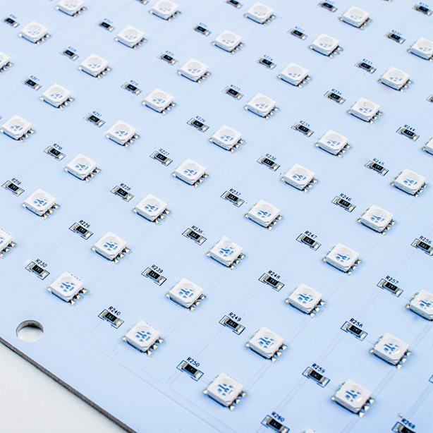
PCB assembly, short for Printed Circuit Board assembly, is the process of populating a printed circuit board with electronic components, such as resistors, capacitors, integrated circuits, connectors, and more, to create a functional electronic device or system. PCB assembly involves several stages,......
Send Inquiry
Product Description
PCB assembly, short for Printed Circuit Board assembly, is the process of populating a printed circuit board with electronic components, such as resistors, capacitors, integrated circuits, connectors, and more, to create a functional electronic device or system. PCB assembly involves several stages, including component placement, soldering, and quality control. Here is an overview of the PCB assembly process:
1. Components Procurement:
- Component Sourcing: Electronic components required for the PCB assembly are sourced from various suppliers. These components can be either through-hole or surface-mount devices (SMDs).
- Component Verification: Components are verified for authenticity, quality, and compatibility with the design. Counterfeit or substandard components can lead to performance issues or failures.
2. PCB Fabrication:
- PCB Manufacturing: The printed circuit board itself is manufactured separately from the assembly process. PCB fabrication involves designing the PCB layout, etching copper traces, and adding layers as needed.
- Panelization: Multiple PCBs are often fabricated on a single larger board, called a panel, to improve efficiency during assembly.
3. Stencil Creation:
- A stencil is created for surface-mount component placement. The stencil is typically made of stainless steel or other materials and is used to apply solder paste to the PCB.
4. Component Placement:
- Pick and Place Machines: For SMD components, automated pick and place machines are used to accurately and quickly position components on the PCB according to the design's specifications.
- Manual Placement: For through-hole components or specialized components, manual placement may be required.
5. Soldering:
- Reflow Soldering: For SMD components, the assembly is typically passed through a reflow oven, where solder paste is melted to form solder joints between components and PCB pads.
- Wave Soldering: Through-hole components are often soldered using a wave soldering machine, which creates a molten solder wave that contacts the component leads and PCB pads simultaneously.
- Hand Soldering: Fine-tuning and rework may require manual soldering by skilled technicians.
6. Cleaning:
- After soldering, the assembled PCB may undergo cleaning processes to remove flux residue and contaminants. Cleanliness is important for the long-term reliability of the PCB.
7. Inspection and Testing:
- Visual Inspection: Trained technicians visually inspect the PCB assembly for soldering defects, misalignment, and component placement issues.
- Functional Testing: The assembled PCB may undergo functional testing to ensure that it operates as expected. This may include electrical testing, firmware programming, and functionality checks.
8. Quality Control:
- Quality control measures are in place to ensure that the PCB assemblies meet the required standards and specifications.
- Any defects or issues identified during inspection and testing are addressed through rework or corrections.
9. Packaging and Shipping:
- After passing quality control checks, the PCB assemblies are packaged and prepared for shipment to their destination, whether it's a manufacturer's production line or end customers.
PCB assembly is a critical step in the manufacturing of electronic devices and systems. The process requires precision, attention to detail, and adherence to industry standards to produce reliable and high-quality electronic products. Different PCB assembly techniques may be used depending on the complexity of the design, the type of components involved, and the volume of production.


